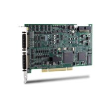
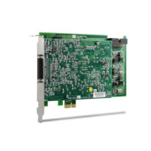
ADLINK’s PCIe-7360 is a high-speed digital I/O board with 32-CH bi-directional parallel I/O lines. Data rate up to 400 MB/s is available through the x4 PCI Express® interface. Clock rate can support up to 100 MHz internal clock or 200 MHz external clock, ideally suiting applications of high-speed and large-scale digital data acquisition or exchange, such as digital image capture, video playback and IC testing.
I/O Port Configuration & Level Shifting
The PCIe-7360, in initial power-up status for onboard 32-channel I/O lines is input lines. The 32-channel I/O lines are bidirectional and can be divided into four groups, each carrying 8 channels and individually configurable as an input or output port. The PCIe-7360 also supports software selectable logic levels of 1.8 V, 2.5 V, and 3.3 V, with all four groups matching the chosen logic level. In digital output mode, the outputs are tri-stated when the digital output lines are disabled. The programmable I/O direction and logic levels provide a flexible interface for devices under test (DUT).
Maximum Data Transfer Rate
The PCIe-7360 can support up to 400 MB/s throughput along with a 32-bit data width at a maximum 100 MHz internal clock rate or 8/16-bit data width at a maximum 200 MHz external clock rate. The combination scatter-gather busmastering DMA, deep onboard 8 k-sample FIFO size, and x4 PCI Express® interface guarantee no data loss during sustained high-speed data processing.
Phase Delay
The PCIe-7360 features phase shifting of external sample clock or internal sample clock exporting, optimizing acquisition/generation timing in high-speed data transfer applications. The phase shifting of sample clock supports adjustment up to 80 steps, that is phase shifting from 4.5¢X to 355.5¢X, preventing erroneous sampling during transition states, such that sample timing is valid and stable.
12C & SPI Serial Interfaces
PCIe-7360’s application function I/O (AFI) can be configured as a I2C or SPI master node. The I2C interface supports fast mode and uses two bi-directional lines, SCL (serial clock) and SDA (serial data) respectively. The SPI interface uses four-wire signaling based on SCK (serial clock), SI (serial data input), SO (serial data output), and CS (chip select). Peripheral devices can communicate directly via the PCIe-7360¡¦s built-in I2C or SPI protocols along with provided APIs.